28.10.10

Free Air Frequencies of Cordless Phones

In the United States, seven frequency bands have been allocated by the Federal Communications Commission for uses that include cordless phones. These are:
  • 1.7 MHz (1.64 MHz to 1.78 MHz & up to 5 Channels, AM System)
  • 43–50 MHz (Base: 43.72-46.97 MHz, Handset: 48.76-49.99 MHz, allocated in 1986 for 10 channels, and later 25 Channels, FM System)
  • 900 MHz (902–928 MHz) (allocated in 1990)
  • 1.9 GHz (1880–1900 MHz) (used for DECT communications outside the U.S.)
  • 1.9 GHz (1920-1930 MHz) (developed in 1993 and allocated U.S. in October 2005)
  • 2.4 GHz (allocated in 1998)
  • 5.8 GHz (allocated in 2003 due to crowding on the 2.4 GHz band).
1.7 MHz cordless phones were the earliest models available at retailers, generally identifiable by their large metal telescoping antennas. Channel selection had to be done manually by the user, and transmitted just above the AM broadcast band. These models are no longer in production, and are considered obsolete due to being very susceptible to eavesdropping and interference, especially from fluorescent lighting and automobile ignitions.
43-50 MHz cordless phones had a large installed base by the early 1990s, and featured shorter bendable antennas plus auto channel selection. Due to their popularity, an over crowding of the band led to an allocation of additional frequencies, thus manufacturers were able to sell models with 25 available channels instead of just 10 channels. Despite being less susceptible to interference, these models are no longer in production and are considered obsolete because these frequencies are easily heard on practically any radio scanner. Advanced models began to use voice inversion as a basic form of scrambling to help limit unauthorized eavesdropping.
900 MHz cordless phones are still sold today and have a huge installed base. Features include even shorter antennas, up to 30 auto selecting channels, and higher resistance to interference. Available in three varieties; analog, digital, and digital spread spectrum, with most being sold today as budget analog models. Analog models are still susceptible to eavesdropping, However, older used models can still be found that are fully capable of receiving this spectrum. Digital variants can still be scanned, but are received as a digital hiss and therefore are difficult to eavesdrop upon. Digital transmission is immune to static interference but can experience signal fade (brief silence) as the phone goes out of range of the base. Digital Spread Spectrum (DSS) variants spread their signal over a range of frequencies providing more resistance to signal fade. The FCC only allows DSS model phones to transmit at the full power of 1 watt, which allows increased range over analog and digital models.
Virtually all telephones sold in the US use the 900 MHz, 1.9 GHz, 2.4-GHz, or 5.8 GHz bands, though legacy phones can remain in use on the older bands. There is no specific requirement for any particular transmission mode on 900, 1.9, 2.4, and 5.8, but in practice, virtually all newer 900 MHz phones are inexpensive analog models with digital features such as DSSS and FHSS generally available only on the higher frequencies
Some cordless phones advertised as 5.8 GHz actually transmit from base to phone on 5.8 GHz and transmit from phone to base on 2.4 GHz or 900 MHz, to conserve battery life inside the phone.
The recently allocated 1.9 GHz band is used by the popular DECT phone standard and is considered more secure than the other shared frequencies

11.10.10

Building a simple USB Charger


A simple USB Charger

USB charging is currently the most universal method of charging an electronic device. This article details the process of construction of a cheap and simple USB charger which can be used to charge cell phones, iPods, mp3 players, cameras, etc and almost any device charges through an USB port of your computer.
USB normally contains 4 lines – Vcc(+5V), Data-(D-), Data+(D+) and Gnd(Ground) . The Vcc and the Gnd line are used to power a device and the D- and D+ line are used to transfer data between the host and the device. A USB standard compliant host is expected to maintain 5V within a range of ± 0.5V and provide current of 1 unit load (I unit load = 100mA of current), unless requested for more current. To build a USB charger all you need to do is build a circuit that outputs current within the USB specification.
The Power Source
Choosing a power source will be the first step in building the charger. There are quite a few options available here. One option is to use 2 AA or AAA size batteries that output 2.4V and boost up the voltage to 5V. These batteries are quite popular and easy to find and they occupy less space and contribute a lot in making the charger small and portable. But they have drawbacks – I have one such charger that really heats up within minutes of connecting it to any device and the worse still, the batteries don’t last longer than than 4-5 minutes.
Another option is to use a pack of 4 Ni-Mh batteries. 4 Ni-Mh batteries output something around 5V depending on their charge. Hence, they can be connected directly to the power pins of the USB port. But the drawback is that 4 Ni-Mh batteries occupy a lot of space and they output voltage based on the amount of charge remaining in them.
Note: If you are using Ni-Mh batteries I would suggest you to use batteries of capacity greater than 2000 mAh. Ni-Mh batteries, though rated at 1.2V, output something around 1.4V when fully charged and 1V when fully drained. This variation is most for Ni-Mh batteries of low capacity(less than 1000 mAh ) and least for batteries of high capacity(greater than 1500mAh). A 2000mAh battery will output 1.3V when fully charged and 1.1V when fully drained.
Another popular power source is a 9V battery. The advantage is it is easily available and cheap. The drawback though is - you will have to regulate the 9V to 5V and only then supply it to the device.
For my charger, I will be making use of a 9V battery and also provide an option for connecting 4 Ni-Mh battery pack to be used as the source.

Voltage Regulation
For voltage regulation, the popular linear LM7805 regulator can be used because – it outputs a constant of 5V, is widely available and comes cheap. The only problem is that there will be a lot of energy wastage if the 7805 is used. The 7805 regulates voltage by converting the input voltage to 5V and the rest to heat. In the process of charging a USB device at 5V by providing it a current of 100 mA, the 7805 will be wasting 0.1*(9 - 5)W =0.4W and have efficiency of( 5V/9V) 55% !(In reality the efficiency is much more because the 9V battery will provide 9V only for the first few minutes and then slowly over time drop down its output voltage to nearly 6.8V before draining completely).
But still I went ahead with using the 7805 because I wanted my charger to be a simple and cheap (efficiency was quite low in my list of priorities). Actually charging any battery with another battery is itself not efficient because you will have wasted energy in charging your source battery and again will be wasting some more energy when charging your USB device’s battery through the source battery!

What about the D- and the D+ lines?
Just providing a 5V across the Vcc and Gnd lines will charge almost most USB device but it is not the best way of charging the device. By just providing a 5V across Vcc and Gnd lines and leaving the D- and D+ lines unconnected (technically called floating) will charge the device at only 100 mA. Charging a battery at 100 mA is a slow process. Hence, we have to tell the device that it has been connected to a charger and that the charger can provide more current. Unfortunately, there is no standard way of doing this and what works for one device does not work for another. For most devices, connecting the D- and D+ lines to 5V through a 100K resistor works. For, charging iPods, the D- line has to connected to 5V through a 10K resistor and the D+ line has to be connected to Gnd through a 10K resistor.

The Circuit
Here is the circuit for charging any USB device –
A simple USB Charger

Here is the circuit for charging an iPod –
A simple USB iPod Charger


Construction
The pictures of the charger I built is shown below (I added a 8mm High Brightness White LED to the board as I had a little space left on the board and didn’t want to waste the space).
A simple USB Charger


A simple USB Charger

You will have to attach a heat sink to the 7805 if you want to charge your device with more than 500 mA of current. Optionally, you can place a 0.1uF capacitor across the power pins of the USB connector as close to it as possible to reduce any noise in the power lines.

25.9.10

Processing explanation of Ultrasonic Range Meter

    This range meter detects a reflected wave from the object after sending out a ultrasonic pulse.
    By measuring the time which returns after emitting a sound wave, a distance to the object is measured.
    The operation of the following figure is repeatedly executed.
    LED display processing is executed in parallel with this operation.
    Label definition
    ;**************** Label Definition ********************        cblock  h'20's_count                         ;Send-out pulse count adr
    endc
    I used CBLOCK directive for the definition of the workarea.
    When using this directive, workareas which were defined between CBLOCK and ENDC are automatically allocated in the order from the address which was specified by the operand of CBLOCK. It is convenient because it is possible to prevent the double allocation of the area. To confirm an allocated address, you confirm it by the assembly result.
    Lighting-up segment data for 7 segments LED are designated by EQU.
    The data from 0 to 9 is used for digital display. However, the 10th is used for the detection error display.
    At first, I make light up only center segment. But I turned off all segments because the display was confusing.
    The 11th is used for the interruption error display. It is for the debugging.
    Environment designating and others
    The following specification is done as configuration word.
    Oscillator
    :
    HS
    Watchdog Timer
    :
    OFF
    Power-up Timer
    :
    enabled
    Low Voltage ICSP
    :
    OFF
    (RB3 can not be used for the input/output port when not making this OFF).
    The result is 3F72h.
    Initialization process
    ;****************  Initial Process  *********************
    Port initialization
    Because the RA0/AN0 port is used for input of A/D converter, it is set to input mode. Other A ports are set to the output. All B ports are set to output because it is used for the LED segment control.
    RC2/CCP1 of C port is set to the input mode because it is used for input of capture.
    Ultrasonic transmission period timer(TMR0) initialization
    The transmission period of the ultrasonic is controlled using timer0. Because timer0 is a timer with byte, the count value is up to 256. However, it is making count 65535 by setting the prescaler to 256. (256 x 256 = 65535) This time, because it is using 4 MHz for the oscillator, 1 count is 1 microsecond. (1/(4 x 106))x4=10-6 seconds
    So, the time-out time of timer0 is about 65 milliseconds.
    Capture mode initialization
    Timer1 is used for capture. Timer1 is initialized.
    At the time of the initialization, it makes CCP1 OFF to prevent from a malfunction.
    A/D converter initialization
    Channel 0 is set as the converter input. Because the clock to use this time is 4 MHz, Fosc/8 is set to A/D conversion clock.
    Because the higher rank side of the A/D converted result are used, the storage of the result is made right justification (ADFM=0).
    Because A porta are used for the output of the digit specification of the LED, ports except RA0/AN0 are made digital specification.
    LED display period timer(TMR2) initialization
    Display data for 7 segments LED are set to workarea. The initial value of the display is "the error code".
    The time-out of timer2 is about 10 milliseconds.
    The interruption eable bits of the capture and timer2 are set.
    Interruption initialization
    It makes timer0 interruption, peripheral device interruption, global interruption possible.
    The interruption of the capture and timer2 doesn't occur when not making peripheral device interruption possible.
    By this process, interruption operation is started.
    When the initialization process ends, the interruption is waited for. It executes same address repeatedly.
    Interruption process
    ;***************  Interruption Process  *****************
    Capture interruption, timer2 interruption, timer0 interruption are checked. The kind of the interruption is judged by each interruption flag. After that, it jumps to the corresponding interruption process.
    When the kind of the interruption is unsettled, processing is stopped. To confirm illegal interruption with the actual circuit, an in-circuit simulator is needed. There is a way of resetting but it isn't improved because it does the same operation even if it resets.
    A global interruption enable bit (the GIE bit) is automatically cleared when the interruption occurs. So, the interruption never occurs while processing in the interruption.
    Illegal interruption process
    ;*************** Illegal interruption *****************
    It displays an interruption error to the LED when the illegal interruption occurs.
    This process is the process for debugging and is usable with the other checking, too.
    Interruption ending process
    ;************  END of Interruption Process **************
    As for the software this time, all processing is done by the interruption except the initialization processing. The common registers(W register, Status register) are not used in the interrupted process (Main process). So, the saving and resaving process for them isn't need.
    In the interruption ending process, GIE bit is set by RETFIE instruction to enable interruption.
    Ultrasonic pulse sending-out process
    ;***************  Pulse send-out Process ****************
    In the pulse sending-out process, the following process is done.
    Clear the interruption display
    The interruption flag of TMR0 is cleared. When not clearing this flag, the interruption occurs at once when interruption processing is ended without waiting a regular time-out.
    I clear the count area of timer0 because of the sure operation.
    Check the detection error
    When the detection of the reflected wave isn't done from the pulse sending-out in the last time until the pulse sending-out this time, it means measurement impossible and display is turned off. The previous data is displayed in the measurement impossible condition when not doing this process and the mistake occurs to the measurement.
    Stop the reflected wave detector
    Immediately after letting out a transmission pulse, the influence occurs to the receiver circuit and there is possibility to do wrong detection. To prevent from this, the operation of the reflected wave detector is stopped. The RA4 port is an open type and an external resistor is needed. So, I used RA5.
    Start the capture operation
    The count area of timer1 and the contents of the capture register are cleared. the rising edge detection mode capture is set and a capture interruption enable bit is set. And an interruption flag is cleared because of the sure operation.
    Send-out the 40KHz pulse
    The 40KHz pulse is the pulse which has 12.5 µ-sec as ON time and 12.5 µ-sec as OFF time in 1 cycle.
    Because 4-MHz clock is used at the circuit this time, the instruction execution time is 1 microsecond. So, correct 40KHz can not be sent out. When doing ON, OFF respectively with the 12 µ-sec, it is 41.7KHz. In case of 13 µ-sec, it is 38.5KHz. This time is adjusted by changing the number of the steps in the pulse sending-out processing.
    It is 0.5 milliseconds when sending out 20 pulses. (20pulses x 0.025milliseconds/pulse)
    Take-in the display revision data
    To make operate A/D converter, the GO bit of the ADCON0 register is set. When switching the input channel of A/D converter, after switching the input, about 20 microseconds waiting time is needed. This time, because the input channel is fixed on 0, waiting time isn't necessary. The completion of the A/D conversion is judged by the checking the GO bit. When GO bit is cleared, the conversion is completion. The upper 3 bits is picked up and add 54 as the conversion value.
    Error detection prevention
    A detector is stopped until the influence ends to the receiver after sending out a pulse. I set this time to about 1 millisecond. When few influences occur, it is to be OK even if it is shorter. When many influences occur, it is necessary to make longer.
    Start the reflected wave detection
    After the wrong detection prevention time elapse, it is made a enable condition in the reflected wave detection.
    Capture interruption process
    ;******************  Capture Process ********************
    In the capture interruption process, the following process is done.
    Clear the interruption display
    Capture interruption flag is cleared.
    Distance conversion processing
    The count value of the timer0 which was stopped by the capture operation is proportional to the propagation time of the sound wave. It isn't possible to use for the display just as it is. In the processing this time, division by some value is done and is converted into the distance numerical value.
    For example, I will explaine in case to have been reflected from the 1-m distance.
    In the time that the sound wave goes and returns in 1 m, it is 2m/343m/sec=5831 microseconds in case of 20°C. Because the clock of timer0 is 1µ-sec/count, the value of the timer0 when a capture is done is 5831. It is to be OK if using 58 as the divisor to make display this value as 100(It displays 1 m). The value to take in by the A/D converter is used for a divisor. So, when the temperature is different, the display can be revised if changing the input voltage to the A/D converter. But, because it is changed in the digital, it isn't possible to do fine adjustment.
    Display setting processing
    Because the type of distance value which is converted is binary, it can not be displayed on the LED just as it is.
    Binary number is converted into the decimal number and is set to each workarea(100th, 10th, 1st).
    When 100th digit exceeds 9, it makes error display.
    LED display process
    ;****************  LED display control  *****************
    This is the process to display the distance numerical value which was gotten by the capture to the LED.
    One LED is controlled at each period. So, only 1 digit is displayed at the same time.
    Display is done every 10 milliseconds using timer2. When the display flickers, you should make the set value of timer2 more little and it quickens a period.

Circuit explanation for Ultrasonic Range Meter

    Receiver circuit
    Signal amplification circuit
    The ultrasonic signal which was received with the reception sensor is amplified by 1000 times(60dB) of voltage with the operational amplifier with two stages. It is 100 times at the first stage (40dB) and 10 times (20dB) at the next stage.
    As for the dB (decibel), refer to "Logarithm Table".
    Generally, the positive and the negative power supply are used for the operational amplifier. The circuit this time works with the single power supply of +9 V. Therefore, for the positive input of the operational amplifiers, the half of the power supply voltage is appied as the bias voltage. Then the alternating current signal can be amplified on 4.5V central voltage. When using the operational amplifier with the negative feedback, the voltage of the positive input terminal and the voltage of the negative input terminal become equal approximately. This is called virtual grounding. So, by this bias voltage, the side of the positive and the side of the negative of the alternating current signal can be equally amplified. When not using this bias voltage, the distortion causes the alternating current signal. This technique is often used when using the operational amplifier which needs two kinds of powers in the single power.
    As for the operation of the operational amplifier, refer to "Operation explanation of the triangular wave oscillator".
    Detection circuit
    The detection is done to detect the received ultrasonic signal. This is the half-wave rectification circuit with Shottky barrier diodes. The DC voltage according to the level of the detection signal is output to the capacitor behind the diode. The Shottky barrier diodes are used because the high frequency characteristic is good.
    As for the Shottky barrier diode, refer to "Diodes".
    Signal detector
    This circuit is the circuit which detects the ultrasonic which returned from the measurement object. The output of the detection circuit is detected using the comparator. At the circuit this time, the operational amplifier of the single power supply is used instead of the comparator. The operational amplifier amplifies and outputs the difference between the positive input and the negative input.
    In case of the operational amplifier which doesn't have the negative feedback, the output becomes the saturation state by a little input voltage. Generally, the operational amplifier has over 10000 times of mu factors. So, when the positive input becomes higher a little than the negative input, the difference is tens of thousands of times amplified and the output becomes the same as the power supply almost.(It is the saturation state) Oppositely, when the positive input becomes lower a little than the negative input, the difference is tens of thousands of times amplified and the output becomes 0 V almost.(It is in the OFF condition) This operation is the same as the operation of the comparator. However, because the inner circuit of the comparator is different from the operational amplifier, the comparator can not be used as the operational amplifier.
    At the circuit this time, the output of the detection circuit is connected with the positive input of the signal detector and the voltage of the negative input is made constant.
    Vrf
    = ( Rb x Vcc )/( Ra + Rb )

    = ( 47K-ohm x 9V )/( 1M-ohm + 47K-ohm )

    = 0.4V
    So, when the rectified ultrasonic signal becomes more than 0.4 V, the output of the signal detector becomes the H level (Approximately 9V).
    This output is lowered with the resistor to make fit with the input of signal holding circuit (TTL:0V to 5V).
     
    Signal holding circuit
    This is the holding circuit of detected signal. SR ( Set and Reset ) flip-flop is used. For the details of SR-FF, refer to "The operation explanation of the D-type flip-flop".
    The detector is made to be not operate in the constant time(About 1.5 milliseconds) after sending out a transmission pulse to prevent from the wrong detection which is due to the influence of the transmission pulse. This operation is controlled with the software of PIC.
    When using the capture feature of PIC, this circuit isn't indispensable. Capture operation is done by the change of the capture input in the once. The reason why I am using this circuit is to confirm signal detection operation within the reflected signal detection time(About 65 milliseconds). When sending out next ultrasonic pulse, the output of this circuit is checked. And when the output is L level, an error display is done because the reflected signal could not be detected.
    Transmitter circuit
    The inverter is used for the drive of the ultrasonic sensor. The two inverters are connected in parallel because of the transmission electric power increase.
    The phase with the voltage to apply to the positive terminal and the negative terminal of the sensor has been 180 degrees shifted. Because it is cutting the direct current with the capacitor, about twice of voltage of the inverter output are appied to the sensor.
    The power supply voltage of this drive circuit is +9V. It is converting voltage with the transistor to make control at the operating voltage of PIC(+5V). Because C-MOS inverters are used, it is possible to do ON/OFF at high speed comparatively.
    7 segment LED display circuit
    Three 7 segment LEDs are used for 3-digit display. As for the lighting-up of the LED, 1 digit is displayed in the order with the software of PIC.
    At the circuit this time, I make light up it when the terminal of PIC is L level. So, ANODE COMMON type is used as the LED. The anode common type is the type which the side of the positive(Anode) of the LED is connected inside. It lights up when grounding(L level) a cathode in the segment to want to make light up.
    As the 7 segment LED, the others have a cathode common type. When you buy them, the specification of the type should be checked.
    Temperature revision voltage generating circuit
     
    The sound wave propagation speed in air is changed by the temperature. At 0°C, it is 331.5m/sec. At 40°C, it is 355.5m/sec.
    For the details of the propagation speed, refer to "The sound wave propagation speed in the air".
    This range meter calculates a distance by dividing the propagation time which was measured by the capture feature.
    I will explain that it does the case of the distance measurement of 1m in the 0°C environment as for the example. The time which the sound wave takes to go and return is 2m/331.5m/sec = 0.006033 seconds = 6.033 milliseconds. The contents of the counter by the capture feature is 6033 within 1 microsecond.
    For the conversion of this to distance (cm), it divides by 60. It is 6033/60=100.55. The following of the decimal point is cut off. It becomes a measurement error.
    This conversion value (60) depends on the temperature. It isn't related with the distance to measure. In case of 9 m, it is 54298/60=904.9. The conversion error becomes big when the distance becomes long. This is because it isn't possible to do conversion below the decimal point.
    In case of 40°C, it is 2m/355.5m/sec = 5625 microseconds and the conversion value is 56.
    The conversion value should be changed by the ambient temperature.
    At this range meter, a conversion value is generated using the A/D conversion feature. The A/D converter converts input voltage into the 10-bit digital data. This time, I am using upper 3 bits. So, the A/D conversion result from 0V to 5V is the value from 0 to 7. And 54 is added to this value.
    Then, the conversion value range is from 54 to 61.
    Resonator
    I used 4-MHz resonator.
    I used 4 MHz in the relation of the timer in the count time. When using 4-MHz clock, it is 1 microsecond per count for the counter count up time. Timer1 to use for capture is a maximum of 65535 counts(16 bits). So, a maximum of 65.535 milliseconds count is made.
    The propagation speed of the sound in air is 343 m/second in case of 20°C. In the time which goes and returns in the 10-m distance, it is 20m/343m/sec = 0.0583 seconds (58.3 milliseconds). As the range meter this time, it is an exactly good value.
    Power supply circuit
    The voltage of +5V and +9V are made with +12V power supply using the 3 terminal regulator.
    +9V are used for the transmitter and the receiver. 100-mA type is used because few needed electric currents.
    In other circuit, +5V is used. +5V voltage is used for the lighting-up of LEDs, because they are controlled by PIC. The about 10-mA electric current per segment flows through the LED. So, it becomes about 80 mA when all segments(eight) light up.
    Because few electric currents of the other IC occur, I think that you can use a 100-mA type, too. I used a 1A type for the safety.

Ultrasonic Range Meter (Circuit Diagram)

26.8.10

Speaker Driver {Special Companies}


HiVi is a leading manufacturer of stereophile quality audio systems. Employing some of the worlds’ finest electro-acoustical technicians and craftsmen, the company established state-of-the art R+D facilities in Toronto, Canada in 1994 and was fueled by early successes with innovative driver designs. In 1997, HiVi merged with highly-regarded speaker manufacturer Swans Speaker Systems and opened corporate offices in Monterey Park, California. Respected audio designer Frank Hale, former president of Swans, continues to serve today as Chief Designer for HiVi Speaker Systems.
HiVi’s proprietary driver technologies including Planar Ribbon Tweeters are employed by many of the audio industry’s top brands. With focused re-investment in research and development, HiVi continues to advance the art and science of electro-acoustical engineering. The merger with Swans provided the opportunity for complete system research and design.
HiVi’s range of drivers and complete speaker systems have been established in niche European, Asian and North American markets for more than a decade. HiVi wholly owns 300 retail stores across Asia, with direct retail presence in an additional 700 locations. With critical success has come substantial growth, and HiVi’s markets continue to expand globally. The HiVi product range has also grown to serve these markets to include high-quality car audio systems, custom home installation speakers and multi-media systems along with home theater systems and drivers.
HiVi founder and president Hong Bo Yao continues to drive the company to new heights. Ongoing research and development programs continue to produce innovative products and technologies - raising the bar on what is possible in high-quality audio reproduction. HiVi is capitalizing on these technologies and extending product offerings successfully into new markets and new categories - converting listeners to audiophiles with uncompromised excellence.

8.6.10

PHASE SEQUENCE DETECTOR {CIRCUIT LOGIC}


In a three-phase system, three circuit conductors carry three alternating currents (of the same frequency) which reach their instantaneous peak values at different times. Taking one conductor as the reference, the other two currents are delayed in time by one-third and two-thirds of one cycle of the electrical current.
The circuit logic is based on this phase difference. The first supply line, line L1, is taken as reference and is called R phase. Now the microprocessor checks which line reaches its peak value next, L2 or L3. If it’s L2 second line is called Y phase and the sequence is RYB. If it’s L3 then third line is Y phase and the phase sequence is RBY. 

5.6.10

PHASE SEQUENCE DETECTOR {Abstract}

The instrument presented here, the PHASE SEQUENCE DETECTOR WITH MOTOR ROTATION SELECTOR permits the electrical contractor or industrial maintenance electrician to permanently connect and tape the terminals of the motor being installed, without having to first energize the motor by a temporary hookup from a power source, if available, to determine motor rotation.
 Therefore, this relay instrument eliminates the need for temporary connections that can be time consuming, costly and quite hazardous, particularly where many large, high-voltage motors are involved. Also, certain types of drives should never be rotated in the wrong direction. In such cases, the temporary hookup or trial method, having a fifty-fifty chance of being wrong, can do serious harm. 

31.5.10

Basic Visible and Infrared Light Detectors

      This page features basic, visible light photo-detector circuits that can be used to detect trains or other light blocking objects.
      The sensors used for these circuits are silicon phototransistors or Cadmium Sulfide (CdS) photocells. Both of these sensors allow less current to flow when they are dark. (Phototransistors change their 'conductance' while photocells change their resistance depending on the intensity of the light falling on them.)
      The phototransistor or photocell would normally be placed between the rails in the circuits on this page.
      The Photo-detectors on this page use LM339 (Quad) or LM393 (Dual) voltage comparator, integrated circuits to detect the change in voltage across the sensor. 
      All of the circuits on this page are configured to have the LED's turn on when the sensor element is dark (covered by a train.) The LED's can also be made to turn off when a train is detected. This will be explained in the NOTES sections of this page.
      The supply voltage for the circuits is specified as regulated 12 volts DC but this can be changed if needed. In some cases the values of some resistors may have to be adjusted to compensate.
    - Section 1 -
    Visible Light Photo-Detector Circuits
    Basic Phototransistor Detector
      In this circuit, when the light falling on the phototransistor (Q1) is blocked, its conductance will decrease and the voltage across Q1 will rise. When the voltage rises above 1/2 of the supply voltage the output of the comparator will turn ON and the LED will be lit.
    Basic Phototransistor Detector
      The only critical part of this circuit is the value of resistor R1 which in most cases can be 470K ohms but may have to be increase if the room is dark or decreased if the room is well lit.
      Increasing the value of R1 will cause the sensitivity of the sensor to decrease. This may be necessary when the light falling on the cell is not very strong or shadows can affect the phototransistor.
      There are a number of phototransistors sizes and case styles. The smaller cases will be easier to hide but connecting wires may be more difficult.
    Basic CdS Photocell Detector
      In this circuit, when the light falling on the photocell (PC 1) is blocked, its resistance will increase and the voltage across PC 1 will rise. When the voltage rises above 1/2 of the supply voltage the output of the comparator will turn ON and the LED will be lit.
    Basic Photocell Detector
      Due to wide variations in CdS photocells it is usually best to install the cell and then measure its resistance under normal lighting conditions. A resistor with a value that is approximately 3 to 5 times the measured resistance of the cell is then selected for R1. For example; If the cell resistance is measured at 400 ohms then a 1200 to 2200 ohms resistor would be used.
      Increasing the value of R1 will cause the sensitivity of the sensor to decrease. This may be necessary when the light falling on the cell is not very strong or shadows can affect the photocell.
      This circuit can be adapted for use in dark areas by placing a small light above the photocell. 
    - Section 2 -
    Infrared Light Photo-Detector Circuit
    Basic Phototransistor Detector
      In this circuit the light falling on the phototransistor will be from an Infrared Light Emitting Diode (IrLED) but otherwise it is the same as the phototransistor circuit shown above.
      When the light falling on the phototransistor (Q1) is blocked, its conductance will decrease and the voltage across Q1 will rise. When the voltage rises above 1/2 of the supply voltage the output of the comparator will turn ON and the LED will be lit.
    Basic Infrared Detector
    Is The IR LED Working?
      Infrared light is not visible to the naked eye, however, a digital camera can be used to view the IR light if it does not have an IR blocking filter on the lens.
      The image may not be very bright but close-up or in a darkened area the light should be visible on the camera's display screen.
    - Section 3 -
    A Practical Quad Photo-Detector Circuit
      The next circuit is for a practical 4 photo-detector circuit using an LM339 Quad comparator IC. Although phototransistors are shown, photocells could also be used with the corresponding change in values for resistors R1 through R4.
      This circuit can also be used for infrared detector circuits as shown above.
    Quad Photocell Detector
      The values for resistors R7 through R10 can also be changed depending on the required LED current. 
      A printed circuit board with 8 comparator type photo-detectors can be seen at this link. 8 Photo-Detector Circuit Board
      This High Impedance Test Voltmeter circuit can also be used for testing phototransistors installations.
    Phototransistor Detector Relay Driver
      By adding a PNP transistor to the basic detector circuit larger currents can be controlled. In this example a small relay is operated by the detector.
    Relay Driver
    Using Multiple Phototransistors
      More than one phototransitor can be connected to a single voltage comparator. This would allow transistors to be placed along a section of track to indicate when a train is anywhere in that section.
      As long as the train is long enough to cover two sensors the circuit will continuously detect the train.
    Multiple Sensors
      Circuit 2 on the schematic is simpler but the phototransistors must have better lighting than Circuit 1 to get good results.

23.5.10

Development Board For PIC & 8051

We are making a new development board for PIC.

It's divided into more parts.
  1. Main board or Microcontroller Board
  2. Real Time Clock board
  3. Relay Board
  4. Stepper Motor Interfacing mode
  5. 4*4 Keypad
  6. LCD interfacing
  7. 16 digit "7-Segment interfacing
  8. Simple status LED board
  9. Temperature controller board
  10. I2C Communication board

21.5.10

Introduction to C and the PIC Microcontroller

Real-World Interfacing

In this lab you will be introduced to the programming language C, and the PIC16F873, a popular and very widely used m-controller (read micro-controller). m-controllers find use in devices that needs some intelligence but not a huge amount of processing power (eg, fancy graphical interfaces, massive computing needs). You can find these devices in cars (engine control, anti-lock brakes...), in appliances, etc... There are many ways to program these devices, but you will be using C to program the PIC to perform some fairly simple tasks. C is often used with m-controllers because of its small size, high speed, and the access it allows to the real-world. This week you will get a short introduction to C as well as a brief look at some of the capabilities of the PIC.
A good resource for help with the PIC programmed with the CCS C-compiler is given at http://www.ccsinfo.com/forum/.
The PIC microcontroller comes in a wide range of variants.  You can check them out in data books that are in the lab, or at the MicroChip web site.  A m-controller is distinguished from a m-processor in that it has many capabilities useful for real-world interfacing built into the chip.  The PIC has a RISC-based Harvard architecture with separate memory for data and program.  The one we will be using is the PIC16F873  (link to data sheet)   It has an on-board RAM (Random Access Memory), EPROM (Erasable Programmable Read Only Memory), an oscillator, a couple of timers, and several Input/Output (I/O) pins, serial ports and 8 channel A/D convertor (if you don’t know what all of those things are don’t worry; suffice it to say there can be an impressive array of peripherals built into the chip). However, the m-controller is less computationally capable than most m-processors due to the fact that they are used for simple control applications rather than spreadsheets and elaborate calculations. As an example, the PIC16F873 has 4096 words of memory for program, and only 192 bytes of RAM, and can only operate with clocks up to 20 MHz on 8 bits of data (compared to megabytes of RAM, Speeds of a GHZ or more and 32 or even 64 bits of data for many desktop systems).  It also has no facilities for floating point numbers... A pinout of the PIC16F873 is shown below.


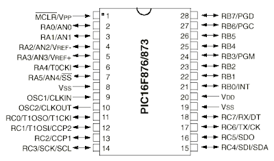
There are several pins that are used to power the device.   Many of the other pins have multiple uses depending on how the device is programmed. 
This week, and the next, you will be using a m-controller in the lab. These laboratories will serve as a brief introduction to the processor and to programming in C.

Getting started with C.
A simple C program
A very simple C program is shown below.
/*simple.c -- sets a pin low, then high*/
#INCLUDE <16F873.h>
#USE DELAY (CLOCK=4000000)
void main() {

        output_low(pin_C1);
        output_high(pin_C1);

}
This program has many common features of C programs. The first line is a comment that is ignored by the compiler.  It is simply there to document what the program code does.  A comment is anything that occurs between a "/*" and the subsequent "*/".  The next line is a "directive".  All directives begin with a "#" and are used to convey information to the compiler.   The directive in this program tells the compiler to include a header file ("16F873.h") which is necessary when using the microcontroller’s input and output capabilities.   The next two directives tell it how to configure the device, and how fast it goes.  The next line tells the compiler that this is the "main" program, and that everything between the opening brace, {, and the matching closing brace, , constitutes the main program. The main program itself is only two lines.   The first  line (not a comment) is a call to the "output_low" function, which sets output pin pin_C1 low, and a call to output_high, which sets it high. . Note that after every program statement there is a semi-colon. This is very important.

Variables
Almost all programs will use variables which are simply units of information stored in the computers memory. The standard C language has a wide variety of variable types available, however the dialect we will be using is more restricted. The version of C that we will be using has a quite unstandard set of variable types that are suited to its architecture.
Type Specifier
Size
Range
unsigned
8 bit unsigned
0 to 255
unsigned int


int


char


int8


long
16 bit unsigned
0 to 65535
long int


int16


signed
8 bit signed
-128 to 127
signed int


signed int8


signed long
16 bit signed
-32768 
to 32767
signed int8


int32
32 bit unsigned
4*109
signed int32
32 bit signed
±2*109
float
32 bit floating point
±0.5*2-128 to 1-(2-15)*2128
short
one bit
0 to 1
short int


int1


The program below shows how variables are used.
#INCLUDE <16F873.h>
#USE DELAY (CLOCK=4000000)
void main() {
   char i, j, k; /* declare characters */
    i=2;
    j=3;
    k=i+j;
}
Again we have a fairly simple program that shows many different features of C. Note the semicolon after every program statement. We declare 3 char’s, "i", "j" and "k".   A char is simply an 8 bit variable.  You should use chars whenever possible because the PIC is designed to work on data 8 bits at a time.

Numerical manipulations
C has a variety of built in operations for performing math. These are listed below along with an example where a=0x03, and b=0x11:

Name of Operand
Symbol
Example
Result a=0x03 b=0x11
Binary Operators (Two Operands)
Addition
+
a+b
0x14

Subtraction
-
b-a
0x0E

Multiplication
*
a*b
0x33

Division
/
b/a
0x05

Modulus
(remainder)
%
b%a
0x02

Bitwise and
&
b&a
0x01

Bitwise or
|
b|a
0x13

Bitwise xor
^
b^a
0x12

Shift right
>>
b>>a
0x02

Shift left
<<
b<
0x88
Unary Operators (One Operand)
increment
++
++a
0x04

decrement
--
--a
0x03

negate
-
-a
-0x03

logical complement
~
~a
0xFC

Logical Expressions
In addition ot manipulating numbers, C is also capable of handling logical expressions. When using these expressions TRUE is taken to be anything that is not zero, and FALSE is always equal to zero. Again, a=0x03, and b=0x11:
Binary operators (two operands)

Name of Operand
Symbol
Example
Result 
a=0x03 b=0x11
Binary Operators
Greater than
>
a>b
FALSE

Less than
<
a
TRUE

Equal
==
a==b
FALSE

Greater than or equal
>=
a>=b
FALSE

Less than or equal
<=
a<=b
TRUE

Not equal
!=
a!=b
TRUE

Logical AND
&&
a&&b
TRUE

Logical OR
||
a||b
TRUE
Unary operators (one operand)
Logical complement
!
!a
FALSE


Manipulating addresses (somewhat advanced topic, may be skipped)
There are two operators used for manipulating addresses and you have already been briefly introduced to one of them, the indirection operator, *. The other one is the address operator &. If you have an address k, the value stored at that address is *k. If you have a variable j, the address of the variable is given by &j. Therefore it is obvious that *(&j)=j.

I/O (Input/Output) Ports
It is possible with with a PIC to interact with the real world.   This is done thourgh the use of I/O ports.  The PIC16F873 has 3 I/O ports, labeled "a", "b" and "c".  We will use Port A for analog input, though it has other uses. Ports B and C will be used for digital I/O.  On the schematic the pins are labeled RB0 through RB7, but the compiler refers to them as pin_B0 through pin_B7.   Likewise for port C.  The pins can be used for either input or output. 
Your circuit has the pushbutton switch connected to RB0, and the LED's to pins RC0 through RC7.
Digital Output
There are several functions that are used for output from the PIC.   A full listing is in the PCB manual.  Four commonly used functions are:
  • Output_high(pin)
    Sets the specified pin to a logic 1 (about 5 volts).
  • Output_low(pin)
    Sets the specified pin to a logic 0 (about 0 volts)
  • Output_float(pin)
    Sets the specified pin to a high-impedance (or tri-state) state.  In this state it is as if the pin has no connections to the chip.  Current can neither go in or out of the pin.
  • Output_bit(pinvalue)
    This function sets the specified pin to the specified value (which must be 0 or 1).
Digital Input
There is only one input function you will need for the PIC.
  • Input(pin)
    Reads the value on a specified pin.  The value is returned in a short int.   A proper use of the function would be something like:

        while( !input(pin_B0)) { ... }

    which would repeat the commands in the braces as long as RB0 was low.
"High level" I/O
If the PIC is connected to the PIC C development software via the debugger it is possible to do some higher level input and output.  These  interactions take place via the debugger's "Monitor" window.
You specify that IO is to take place through the debugger by properly defining serial connections (usually in your codes header file):
#use rs232(DEBUGGER)
You can then print to the monitor window by using "putc()" which sends a character to the monitor window, "puts()" which sends a string, or "printf()" which sends a formatted string.  The "printf()" command is most useful, but also the most complicated (and takes the most memory).
The syntax of printf is the following:

printf(format-string, [arg_1] , ... , [arg_N] )
This is best illustrated by some examples.
Example 1: Printing a message. The following statement prints a text string to the screen.

printf("Hello, world!\n");
In this example, the format string is simply printed to the screen.
The character \n at the end of the string signifies end-of-line. When an end-of-line character is printed, the LCD screen will be cleared when a subsequent character is printed. Thus, most printf statements are terminated by a \n.
Example 2: Printing a number. The following statement prints the value of the integer variable x with a brief message.

printf("Value is %d\n", x);
The special form %d is used to format the printing of an integer in decimal format.
Example 3: Printing a character. The following statement prints the ascii equivalent of the integer variable x with a brief message.   Here is an ascii table.

printf("Value is %d, ascii = %c\n", x, x);
Example 4: Printing a number in binary. The following statement prints the value of the integer variable x as a binary number.

printf("Value is %b\n", x);
The special form %b is used to format the printing of an integer in binary format. Only the low byte of the number is printed.
Example 5: Printing a floating point number. The following statement prints the value of the floating point variable n as a floating point number.

printf("Value is %f\n", n);
The special form %f is used to format the printing of floating point number.
Example 6: Printing two numbers in hexadecimal format.

printf("A=%x  B=%x\n", a, b);
The form %x formats an integer to print in hexadecimal.
%d
Type: int Description: decimal number
%x
Type: int Description: hexadecimal number
%b
Type: int Description: low byte as binary number
%c
Type: int Description: low byte as ASCII character
%f
Type: float Description: floating point number
%s
Type: char array Description: char array (string)
Format Command
Data Type
Description
%d
int
decimal number
%x
int
hexadecimal number
%b
int
low byte as binary number
%c
int
low byte as ASCII character
%f
float
floating point number
%s
char array
char array (string)

Your circuit has the pushbutton switch connected to RB0, and the LED's to pins RC0 through RC7.
Input
Unfortunately, you can only receive input from the keyboard one character at a time using the getc() command.  Be aware:
  • getc() returns the ascii equivalent of the character entered into the keyboard.
  • the keyboard I/O is implemented in software on the PIC.  That means, it won't receive input from the keyboard unless it is explicitly looking for it.  Therefore, your program must stop in order to look for input from the keyboard.  (Hardware communications could receive a character in the background, without requiring software support).
As an example, the following code gets the ascii value in k, converts to a number, and prints the number.
k=getc();                %Get ascii value of keyboard input.
k=k-'0';                 %Subtract value of '0' to convert to number.
printf(" ... k=%d\n",k); %print the number.
Control of Flow
What you have learned up to this point has been useful but is of limited utility because it does not allow for decision making capabilities by the computer. C has a variety of mechanisms to control the flow of a program. These are listed below:
The if...then construct
if (logical expression) {
    ...statements...
}
If the logical expression is true then evaluate the statements between the braces. The following code sets RC1 if a is even.
if ((a%2) == 0) {
   Output_high(pin_C1);
}
The if...then...else construct
if (logical expression) {
   ...if statements...
}
else {
   ...else statements...
}
If the logical expression is true then evaluate the "if" statements between the braces, otherwise execute the "else" statements. The following code decides if a number if is even or odd.
if ((a%2) == 0) {
   Output_high(pin_C1);
}
else {
   Output_low(pin_C1);
}
The while loop
while (logical expression) {
    ...statements...
}
While the logical expression is true, the statments (of which there is an arbitrary number) between the braces is executed. The following code cycles through the even numbers from 0 to 9 (the variables must have been declared elsewhere in the program).
a=0;
while (a<10) {
    ...statements...
    a=a+2;
}

The for loop
for (initial condition; logical expression; change loop counter variable) {
    ...statements...
}
Set the initial condition, then while the logical expression is true execute the statement between the braces while changing the loop counter as specified once at the end of each loop. This code segment is functionally equivalent to the one for the "while" loop.
for (a=0; a<10; a=a+2) {
    ...statements...
}

The case...switch construct
Case..switch is used in place of a series of "if...else" clauses when a variable can take on several values.  The "default" clause at the bottom takes care of any cases not covered explicitly.
switch (variable) {
   case val1: ...statements 1...
   break;
   case val2: ...statements 2...
   break;
   case val3: ...statements 3...
   break;
   default: ...statements default...
   break;
}

Functions
Often a series of instruction must be repeated over and over again. Instead of repeating the same operations repetitively it is useful to use a function that performs the repetitive operations. For instance to set a value on RC1 and then read from RB0 and set RC0 to that value, and returning the value of RB0 you might use a function called "RB0toRC0".  (Note: this program isn't meant to be particularly useful, but to introduce the syntax for function declaration, and use).
/*simpleFunc.c -- to demonstrate function calls*/
#INCLUDE <16F873.h>
#USE DELAY (CLOCK=4000000)
short int RB0toRC0(RC1val)
short int RC1val;
{
   Output_bit(pin_C1, RC1val);  /*Set RC1 to the specified value*/
   if (input(pin_B0)) {         /*Read RB0*/     
      Output_high(pin_C0);      /*If RB0 is high, RC0 set high*/
   }
   else {
      Output_low(pin_C0);       /*else set RC0 low*/
   }
   return(input(pin_B0));       /*Return RB0*/
}
void main() {
   short int b;

   b=RB0toRC0(1);
   b=RB0toRC0(0);
}
This program introduces some new constructs. The most obvious is the function "RB0toRC0" which is at the top. The first line of the function declares that the function returns a short int, and has one argument. The type of the argument is given before the function's opening brace. The body of the function (between the braces) outputs a value to RC1, and reads from RB0 and echos to RC1.  The last line tells that compiler to return the value of RB0 to the calling function.
The function is called in the main program with different arguments.   The first call would set RC1 high, and return the current value of RB0 to the variable "b".  The next line would set RC1 low, and return the value of RB0 to the variable "b".
Wrapping up
You should now know enough to do some fairly simple things with the microcontroller. This has been a very brief introduction to C and did not even begin to touch the richness available with the language. If you would like to know more look in the manuals in the lab, or some of the books in the library.